Over the last few weeks and months I've been considering headphone amplifier design. After my first attempt at a headphone amplifier, I've wanted to produce something a bit more significant but build on the simplicity of design that the CMoy / Tangent variant offers. I don't know where this thread will end up....and it may peter out after a few posts. However, my ambition is to design a circuit and optimise the circuit through modelling, build a prototype and then design and commission a professional pcb. Another design goal is to make each channel a discrete module to allow passive ground, active ground and balanced topologies to be supported with a single design. The simplest way to build on the CMoy is to use integrated circuit (IC) buffers to boost the output current of the opamp to drive the headphones, thereby minimising the errors and distortion produced by the opamp. Perhaps the best known IC buffer is the Burr Brown (now Texas Instruments) BUF634. The data sheet associated with this buffer includes a design for a high performance headphone driver, so I will use this as my starting point. More to follow.....
DIY Headphone Amp #4 - Design, Modelling and Prototyping
- Thread starter PJPro
- Start date
You are using an out of date browser. It may not display this or other websites correctly.
You should upgrade or use an alternative browser.
You should upgrade or use an alternative browser.
Before looking at the high performance amplifier, I'd like to look at something more basic from the same BUF634 datasheet. This design illustrates how to use a buffer to boost the current from an op amp.
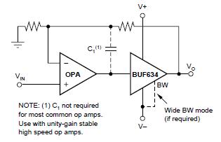
Fig 1: Texas Instruments - Boosting Op Amp Current
Let's consider the design of this non-inverting amplifier.....
The signal enters the circuit at VIN. It enters the non-inverting (positive) pin of the opamp. The signal is amplified as it passes through the chip and exits from the output pin of the opamp (pointy end). This amplified signal now enters the buffer, where the output current is boosted, passes out the output pin (pointy end) and finally exits the circuit at VO.
There is also a feedback loop which connects the circuit output to the inverting (negative) pin of the opamp and to ground. The ratio of the two resistors in the feedback loop are used to control the gain (amount of amplification) applied to the input signal by the Op Amp. The gain is calculated using (right resistor / left resistor) + 1.
The capacitor at C1 can be tweaked to improve the performance of the amplifier. The faster the op amp and the lower the gain, the higher the required value of the capacitor.
V+ and V- are the rails which power the buffer to do its work.
This is just about the most basic design possible with a buffer placed in the feedback loop of an op amp. So why does the buffer feature in the feedback loop rather than after the opamp circuitry? Well, buffers tend to suffer from offset voltages (for offset read error). By placing the buffer in the feedback loop of the opamp, these errors are corrected by the opamp circuitry.
More to follow........
Armed with an understanding of the most basic circuit, we can now move onto the high performance circuit provided by Texas Instruments.
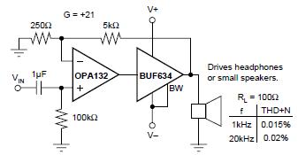
Fig 2: Texas Instruments - High performance headphone driver using the BUF634.
Let's consider the design.....
There's not much additional circuitry over the most basic design.
You'll notice the resistors in the feedback loop have been given values and the gain has been stated, being calculated using (5K / 0.25K) + 1 = 21. From personal experience, that's a massive amount of gain, so I'll be looking to reduce that as our amplifier evolves.
RL has been added to the circuit to represent the load of a speaker or headphone. This will be important when we come to model the design.
The most significant addition to the circuit is a high pass filter, which has been placed on the input side of the op amp. This comprises of an non-polarised input capacitor and a resistor running to ground.
This filter (and in particular the input capacitor) will remove any DC offset which may be in the signal. A well designed source should eliminate/minimise DC offset, so it shouldn't be a problem for us. However, if DC offset is present in the signal, it will be amplified and could potentially damage any attached speaker/headphone. So DC offset is bad, bad, bad.
The downside is that the filter will degrade sound quality by attenuating low frequency signals (creating roll off) and cause phase distortion. Moreover, imperfections in the material of the capacitor can cause further distortions.
There are circuit designs can be used to "deal" with DC offset, e.g. the DC Servo, or disconnect the speakers when DC offset is detected, so that the input capacitor can be omitted. (I intended to use the latter approach for my DIY Dual Mono Power Amps project...I really must finish these). However, these techniques add to the complexity (and expense) of the design.
The high pass filter is simple, effective and is widely used in quality commercial products, like the Graham Slee Novo. So I'm going to adopt the approach and avoid skimping on the quality of the capacitor to minimise signal degradation.
More to follow....


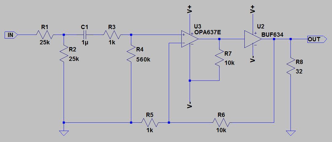

Refering to Figure 3 (above)....
R1 and R2 have been added to represent a 50K Ohm potentiometer (pot). Using two resistors is a simplification for the modelling to follow. The pot attenuates the input signal by varying the ratio of R1 to R2. Together, these resistors form a voltage divider so as R1 gets smaller the attenuation is reduced (and the amp will get louder)
To balance the op amp input impedance, I have added the resistor at R3, selecting a value to equal that of R5. R3 creates a voltage divider with R4, resulting in the attenuation the signal. However, the value of R3 is much lower than R4, so the effect will be minimal.
The value of R4 has been increased to 560K Ohm. The rule of thumb for the value of this resistor is that it needs to be at least 10 times greater than the pot. This leads me to believe the Texas Instruments schematic must have been expecting a 10K pot.
R5 and R6 have been increased to 1K and 10K respectively. R5 provides symmetry with R3. R6 has been selected to provide a gain of 11 i.e. (R6 / R5) + 1 = 11. In my experience, this is still high but it suits the op amp I have selected; the OPA637.
The OPA637 (along with the OPA627) is regarded as being at the audiophile end of the op amp world, with a high-end price to go with it. The data sheet can be found here. This is a high speed, low noise, precision op amp. However, it is unstable below gains of 5, hence the gain of 11 selected above. It will provide a definate improvement in sound quality over the OPA132 but, as already stated, isn't going to be cheap at around £20 each.
The R8 resistor has been added to simulate the load placed on the circuit by the headphones and 32 Ohms reflects the impedance of my Grado headphones. This is required for the modelling to follow.
However, the most interesting addition is the resistor at R7. This resistor serves to bias the op amp into Class A. This means the output stage of the op amp is turned on all the time, resulting in better sound quality. The downside is the op amp is less efficient to run.
Biasing the op amp into Class A using a resistor is the simplest but least effective option we can use, with the most effective being the JFET cascode. I hope to cover this next.
More to follow....
The goal with biasing to Class A is to keep the output stage of the op amp turned on and, to do this, we need to keep the op amp constantly passing more current than it would driving its load alone. For buffered op amp circuits we need to be aiming for a current between approximately 0.5 and 5mA, depending on the op amp being used, its maximum signal voltage and the impedance of the buffer (the load).
Refering to Figure 3 (above), the current through R7 will be stable if the voltage across R7 is stable. However, the signal from the output of the op amp will impact this stability thus the current across R7 will change. Remember, what we are trying to achieve here is a stable current to bias the op amp.
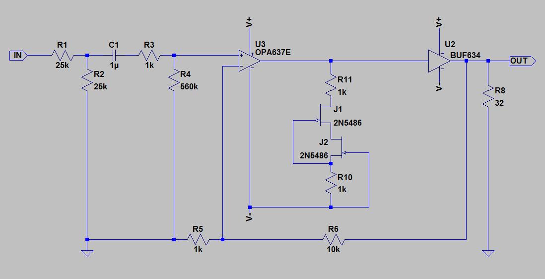
Figure 4: Second Iteration with JFET Cascode.
The JFET cascode provides a superior approach for biasing op amps into Class A. So, what's a JFET? Effectively, it is a voltage controlled resistor. The transistor has three pins; a gate, a source and a drain. The current runs from the drain to the source and is limited by the voltage drop between the gate and source. As the voltage drop varies, so the current allowed to flow is reduced or increased.
I have added a JFET cacode to our schematic (see Figure 4). The two JFETs interact to stablise each other, leading to a near constant current level through the cascode. The resistor at R10 increases this stability further, while the resistor at R11 helps to isolate the op amp from the capacitance introduced by J1.
The 1k resistor at R10 (Figure 4), with a voltage of -15 on the negative rail, results in a current of 3.1mA through the cascode. However, if R10 is replaced with a trim pot, it will allow the current across the cascode to be tuned to achieve a desired level of biasing.
More to follow....
Refering to Figure 3 (above), the current through R7 will be stable if the voltage across R7 is stable. However, the signal from the output of the op amp will impact this stability thus the current across R7 will change. Remember, what we are trying to achieve here is a stable current to bias the op amp.
Figure 4: Second Iteration with JFET Cascode.
The JFET cascode provides a superior approach for biasing op amps into Class A. So, what's a JFET? Effectively, it is a voltage controlled resistor. The transistor has three pins; a gate, a source and a drain. The current runs from the drain to the source and is limited by the voltage drop between the gate and source. As the voltage drop varies, so the current allowed to flow is reduced or increased.
I have added a JFET cacode to our schematic (see Figure 4). The two JFETs interact to stablise each other, leading to a near constant current level through the cascode. The resistor at R10 increases this stability further, while the resistor at R11 helps to isolate the op amp from the capacitance introduced by J1.
The 1k resistor at R10 (Figure 4), with a voltage of -15 on the negative rail, results in a current of 3.1mA through the cascode. However, if R10 is replaced with a trim pot, it will allow the current across the cascode to be tuned to achieve a desired level of biasing.
More to follow....
While researching this project, I stumbled across an application note for the BUF634 on the by Texas Instruments website, written by Burr-Brown. It's called "Combining an amplifier with the BUF634". You can find the application note here. This provides some additional tweaks to our circuit. These have been captured in figure 5 (below), along with some other modifications to the circuit.
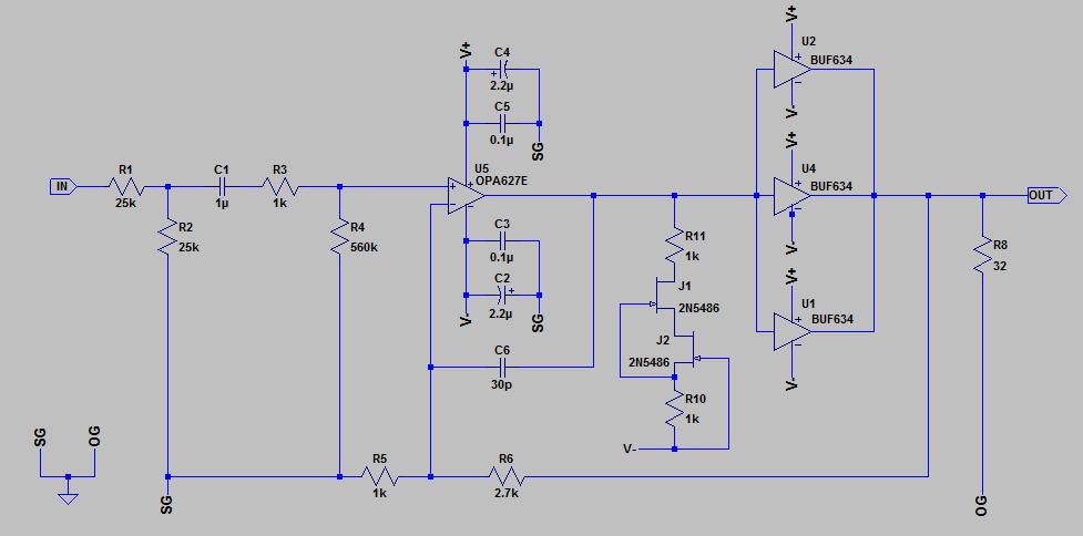
Figure 5: Third Iteration with Multiple BUF634s.
The clear difference between this version of the schematic and the previous version is the addition of two extra buffers. The reasoning is that at high frequencies and loads, the distortion produced by the buffer increases. Increasing the number of buffers in the circuit shares the load and, therefore, reduces distortion at higher frequencies.
The application note recommended a value of 2.7K for our R6 resistor (Rf on their schematic). I have updated R6 to reflect this recommendation, resulting in a gain of (R6 / R5 ) + 1 = (2.7 / 1) + 1 = 3.7.
As previously mentioned, the OPA637 becomes unstable with a gain less than about 5, so I have swapped out the OPA637 for the OPA627. It is claimed that the OPA627 is stable at a gain of 1 (or unity gain), so it should suit our purposes. The OPA627 is also used in the application note.
I have followed the advice regarding the capacitors on the power rails supplying the opamp. You may remember my first DIY headphone amp where oscillation proved to be a problem. This was solved using decoupling caps. C3 and C5 in figure 5 serve the same purpose and help to stablise the opamp.
C2 and C4 provide a store of energy to meet any rapidly changing demand of the opamp i.e they can respond faster than the wider power supply circuit.
You may have noticed that ground (the downward pointing triangle) has been replaced by SG (below R2) and the OG (below R8). These stand for Signal Ground and Output Ground respectively and provide a hint towards a potential grounding solution. For now I have tied these to a common ground (bottom left).
Finally, I have added the capacitor C6 with an arbitary value of 30pF. The need for this capacitor was established in figure 1 and now seems as good a time as any to add it to the schematic.
More to follow........


idc:Any more progress? Any pictures?
Some progress, yes. But not much. I think I have the final design of a channel but still have the power supply to do.
The delay is mainly due to getting my head around the analysis of the circuit as I'd like to show some simulations and demonstrate the use of the SPICE tool. A great leap forward, in this regard, has been my joining of a forum on yahoo.
And after all, I don't want to build an amp that can be shown to be rubbish even under ideal conditions.
PJPro, is this on hold due to a DIY BBQ project or something?

this one sounds like a DIY BBQ may be taking priority!?
PJPro:I'm in the market for a weber but am having difficulty justifying the outlay. They're not cheap.....secondhand or otherwise.
this one sounds like a DIY BBQ may be taking priority!?
PJPro:I'm in the market for a weber but am having difficulty justifying the outlay. They're not cheap.....secondhand or otherwise.
Similar threads
- Replies
- 8
- Views
- 1K
- Replies
- 2
- Views
- 3K
- Replies
- 57
- Views
- 7K
Space.com is part of Future plc, an international media group and leading digital publisher. Visit our corporate site.
© Future Publishing Limited Quay House, The Ambury, Bath BA1 1UA. All rights reserved. England and Wales company registration number 2008885.
 Twitter